Introduction

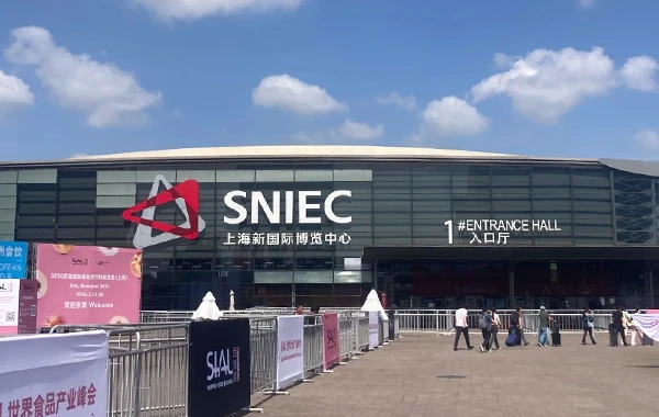
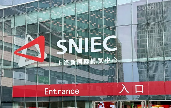
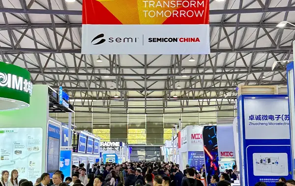
SEMICON China is the most important semiconductor industry event in Asia and one of the largest in the world. Organized by SEMI, the global industry association for electronics manufacturing and design, SEMICON China 2027 takes place March 24-26 at SNIEC. The annual exhibition brings together 1,000+ exhibitors and 100,000+ professionals from across the chip ecosystem -- equipment makers, material suppliers, foundries, OSAT providers, EDA companies, and chip designers. As the world's largest semiconductor consumption market, China is central to the global industry, and SEMICON China is the essential gateway for international companies.

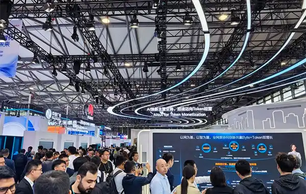
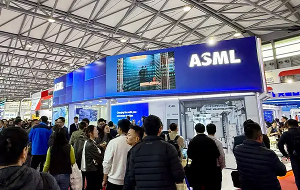
The show floor showcases the technologies powering global electronics. Applied Materials, Lam Research, Tokyo Electron, and ASML demonstrate their latest wafer processing platforms, alongside material suppliers presenting advanced photoresists, specialty gases, and substrate innovations. The concurrent conference features the Opening Keynote with global semiconductor CEOs, the Global Semiconductor Industry Strategy Summit (ISS), and the SEMI Industry Innovation Investment Forum (SIIP China). The co-located CSTIC, jointly organized by SEMI, IEEE, and China's high-tech expert panel, is Asia's largest semiconductor technical symposium running since 2000.

Key Exhibition Areas

Wafer Processing Equipment -- Lithography, etch, deposition, CMP, ion implantation, and thermal systems for front-end manufacturing.

Semiconductor Materials -- Silicon wafers, photoresists, CMP slurries, specialty gases, sputtering targets, and substrates.

Packaging and Test -- Advanced packaging, wafer-level test, probing systems, final test handlers, and ATE platforms.

EDA and Design -- EDA software, IP cores, design services, and verification platforms for chip design.

MEMS and Sensors -- MEMS fabrication, sensor integration, microfluidics, and wafer-level packaging for IoT and automotive.

Power and Compound Semis -- SiC and GaN devices, power ICs, RF semiconductors, and high-voltage manufacturing processes.

Fab Facilities -- Cleanroom construction, AMHS, facility management, and fab automation systems.

Gas and Chemical Systems -- Bulk gas delivery, chemical distribution, exhaust management, and ultra-high purity systems.

IC Design and Foundry -- Fabless design, wafer foundry, MPW services, and chip prototyping platforms.

Supply Chain and Logistics -- Equipment spare parts, refurbished tools, supply chain software, and global logistics for semiconductor manufacturing.

Venue Information

Shanghai New International Expo Centre (SNIEC), Pudong

Address: 2345 Longyang Road, Pudong, Shanghai, China

Hours: March 24-25: 09:00-17:00 | March 26: 09:00-16:00

Transportation: Close to Pudong Airport; accessible via metro Line 7 / Line 2


As a business travel service provider, we offer comprehensive support for international SEMICON China attendees, including visa invitation letters, hotel booking near SNIEC, airport transfers, and guided tours of Zhangjiang Science City's semiconductor cluster. Contact us to plan your SEMICON China 2027 itinerary.

Maybe You Like